
Samsung chief Lee visits Japan chip packaging lab
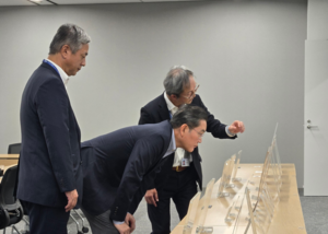
Samsung Electronics Executive Chair Lee Jae-yong visited the company's advanced semiconductor packaging research facility in Japan on Sunday, emphasizing the need to secure cutting-edge packaging technologies to sharpen its competitive edge in AI chips. Lee inspected the Advanced Package Lab in
Samsung Electronics Executive Chair Lee Jae-yong visited the company's advanced semiconductor packaging research facility in Japan on Sunday, emphasizing the need to secure cutting-edge packaging technologies to sharpen its competitive edge in AI chips. Lee inspected the Advanced Package Lab in
💬 留言板 — 歡迎分享你的想法!
登入 Google 帳號即可留言